


ITEM SPECIFICS
-
Brand
HDI PWB
-
origin
Republic of Korea
-
Size(Capacity)
-
-
Color
Green / Blue / Red
-
Material
FR-4
-
Features
Laser drill, Copper filling
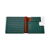
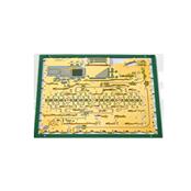
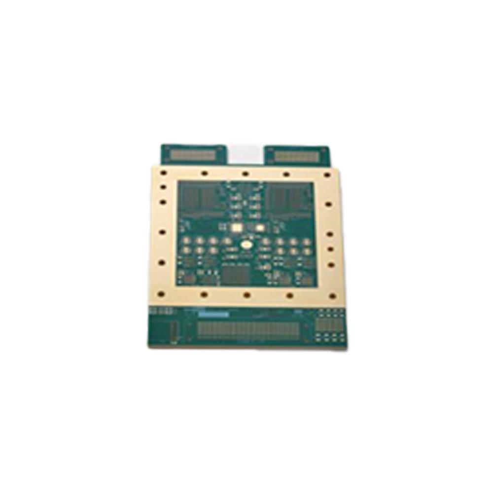
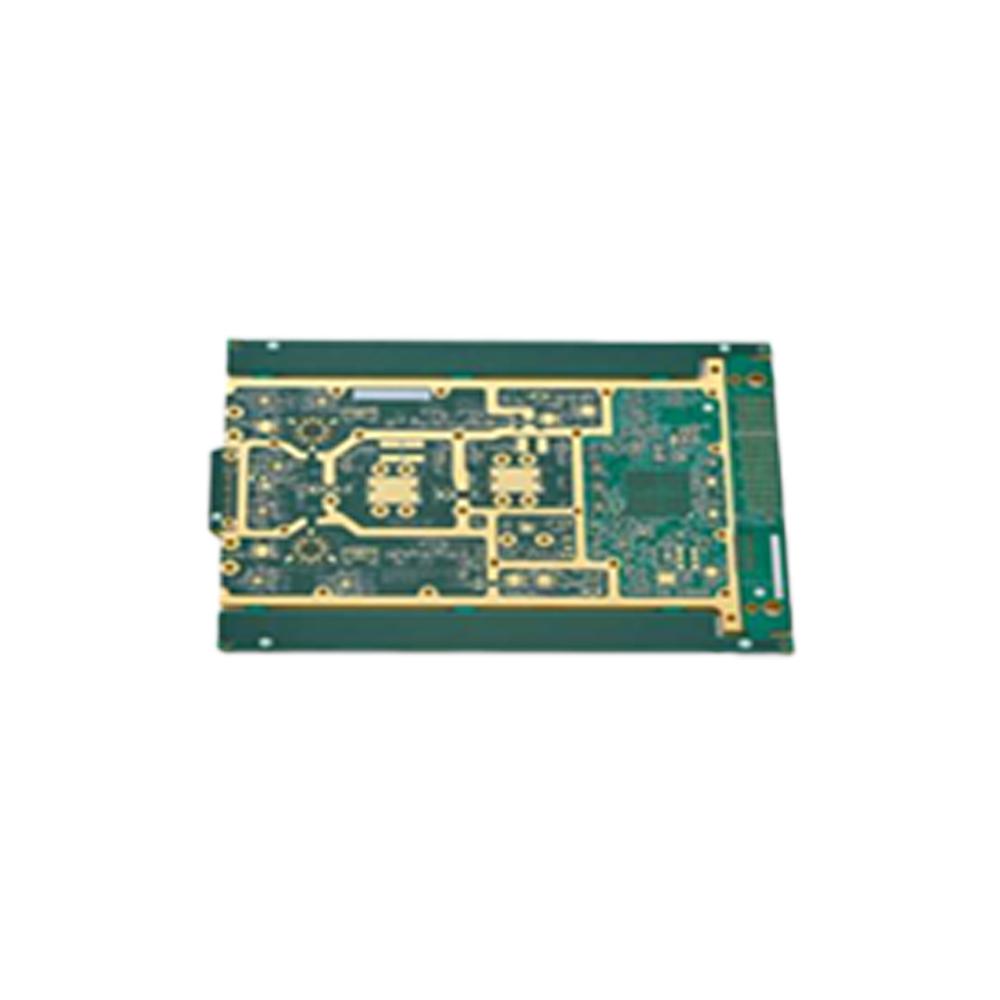
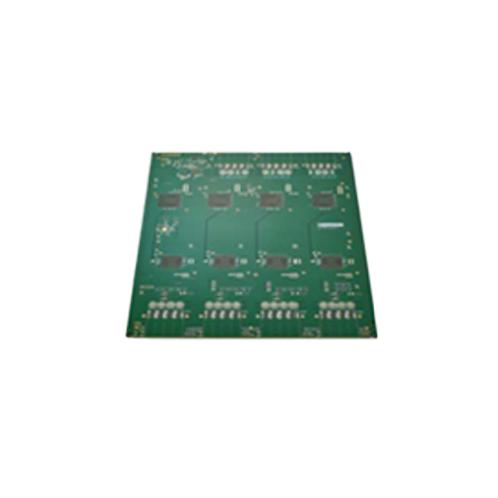
PRODUCT DESCRIPTION
It's for mobile and high tech electronic devices by connecting each x-layer made of fine circuits with laswer micro via to form a more complex and multifunctional wiring structure.
1. Capabilities :
* Stacked microvias ( plated copper ) and staggered microvias
* Cavities, countersunk holes or depth milling
* Solder resist in black, blue, green, etc.
* Low-halogen material in standard and high Tg range Low-Dk material for Mobile Devices
* All recognized printed circuit board industry surfaces available
2. Special Capabilities :
* Copper filling process
* Plated Over Via Filling
3. Application : Network / Military / Medical / Defense / Aerospace
PAYMENTS DETAILS
This supplier supports payments for offline orders
- Telegraphic Transfer : T/T
- Name : KIM, MI-KYUNG
SHIPPING
Shipping from :
Republic of Korea
- Namdong Industrial Complex 67B-1L 628-12 Gojan-dong Namdong-gu Incheon 405-817 Korea, 인천광역시,
EOS CORPORATION.
The person in charge
Address
Namdong Industrial Complex 67B-1L 628-12 Gojan-dong Namdong-gu Incheon 405-817 Korea, 인천광역시,
QR code
EOS CORPORATION.
-
- Business Type :
- Manufacturer
-
- Main Product :
-
- Established :
- 2004-01-01
COMPANY ENVIRONMENT


Please suggest a variety of your ideas such as design, impact, enhancements, etc
Captcha Required
Please enter the text on the left image to prevent automatic input.
0 / 4000
질문이 없습니다.
CUSTOMER REVIEWS (0)

COMPARISON TO SIMILAR ITEMS more
- No Items
- supplier level
-
 GOLD
GOLD
- EOS CORPORATION. Seller's Store
- Seller's Store url
- Response Level
★ ★ ★ ★ ★

- Supplier Level
★ ★ ★ ★ ★
- Transaction Level
★ ★ ★ ★ ★
SUPPLIER BEST